Localize semiconductor defects including depth with high accuracy, non-destructively

Already running in the labs that matter
Our tool is installed and operational at our headquarters in Munich as well as leading FA labs, including EAG Laboratories in San Jose and Integrated Service Technology (iST) in Hsinchu, Taiwan.


We find your hardest failures
Conventional tools see structure. We see the current — so we localize the electrically active faults that hide inside advanced packages and pinpoint the layer, without destroying the sample.
The faults we localize
- Opens
— true, intermittent, soft, and high-ohmic opens, to micron accuracy - Shorts
— metal, RDL, and power-to-ground shorts, including low-ohmic shorts - Leakage
— leakage paths between conductors, even below in-line test thresholds - Current crowding
— current redistribution and hotspots in high-density interconnects - Power-device faults
— oxide issues and current crowding in SiC and GaN devices
Where they hide
- Backside power delivery networks
— read through the full package thickness, no layer removal - 2.5D and 3D stacks
— buried interconnects structural inspection can't reach - Hybrid bonds and TSVs
— interface and via faults inside bonded stacks - Redistribution layers (RDL)
— opens and shorts in fan-out routing - Package-on-package / integrated fan-out
— a backside short localized to ~20 µm in a published case - HBM and high-density memory stacks
— faults inside the stack, non-destructively
We haven't seen a more exciting tool in the past 20 years.

We were looking for a defect for six weeks, and with QuantumDiamonds we found it in 60 seconds.
Failures don't stand a chance
Our application notes come from anonymized, real customer measurements. Start with this case study of our non-destructive failure analysis of an integrated fan-out package-on-package chip.


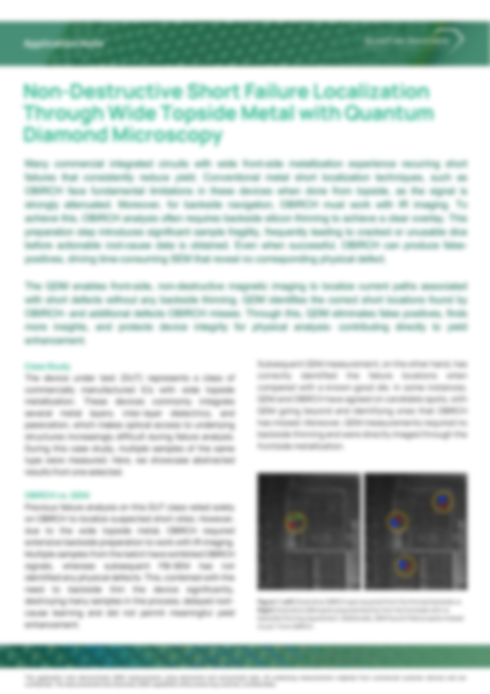
Quantum Diamond Microscopy for Non-Destructive Failure Analysis of an Integrated Fan-Out Package-on-Package Chip
Newsroom

QuantumDiamonds Reaches Key Milestone on the Path to Inline Electrical Inspection with Contact-Free Current Imaging
QuantumDiamonds Reaches Key Milestone on the Path to Inline Electrical Inspection with Contact-Free Current Imaging
QuantumDiamonds Reaches Key Milestone on the Path to Inline Electrical Inspection with Contact-Free Current Imaging
.jpg)
Bavarian Deputy Minister-President and German Federal Ministry for Economic Affairs (BMWE) visit as QuantumDiamonds opens first section of its new Munich production facility
Bavarian Deputy Minister-President and German Federal Ministry for Economic Affairs (BMWE) visit as QuantumDiamonds opens first section of its new Munich production facility
Bavarian Deputy Minister-President and German Federal Ministry for Economic Affairs (BMWE) visit as QuantumDiamonds opens first section of its new Munich production facility
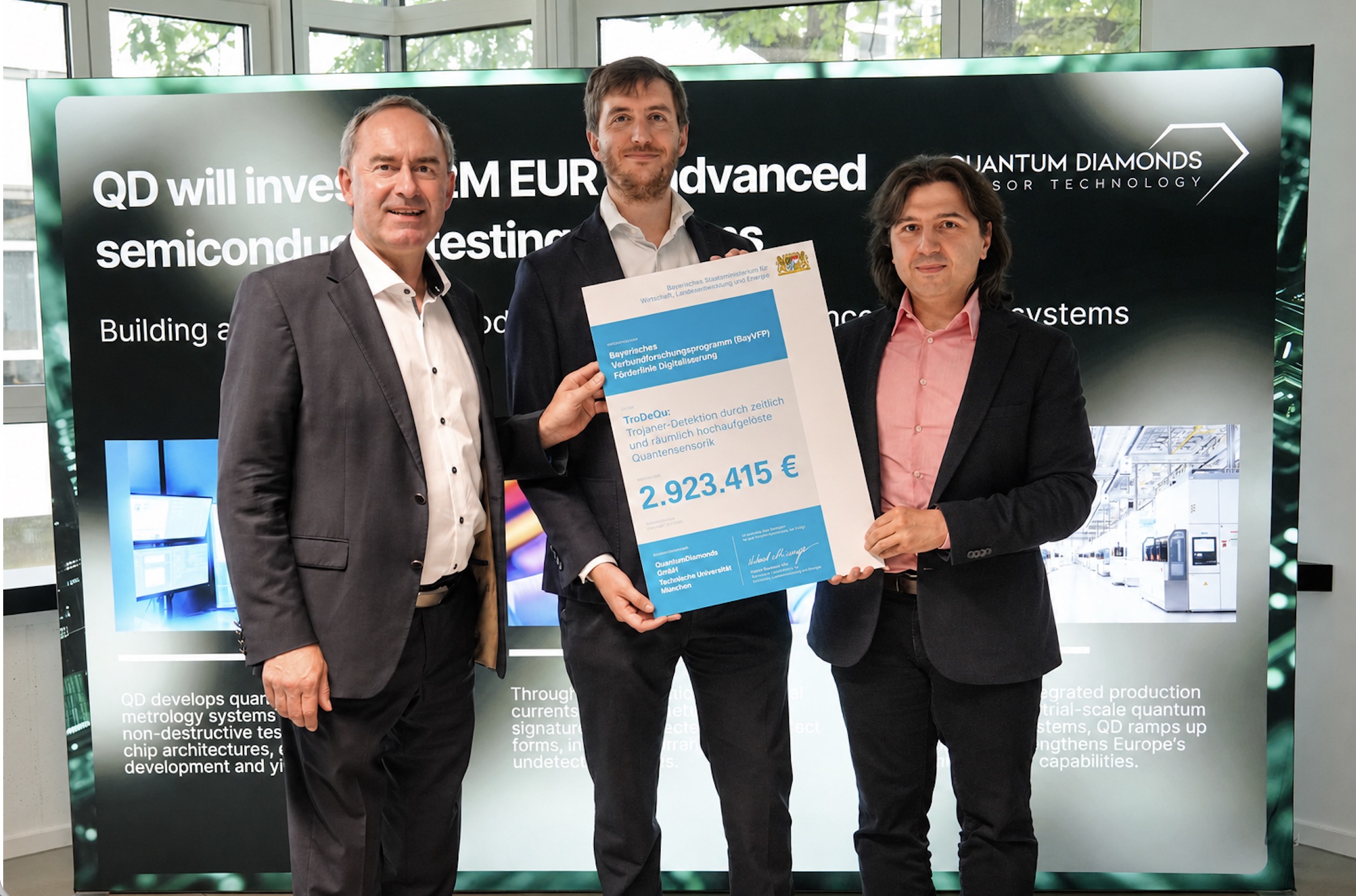
QuantumDiamonds and TU Munich receive funding for TroDeQu, the first European effort to detect hardware trojans with quantum sensing
QuantumDiamonds and TU Munich receive funding for TroDeQu, the first European effort to detect hardware trojans with quantum sensing
QuantumDiamonds and TU Munich receive funding for TroDeQu, the first European effort to detect hardware trojans with quantum sensing
Ready for today. Ready for tomorrow.
QuantumDiamonds develops and deploys next-gen semiconductor testing tools for the advanced packaging era, while offering in-house failure analysis with quantum sensing as a service.

In-Lab
Commercially available, reach out for more information
High-resolution, non-destructive localization of defects at the single-chip level for R&D and failure analysis.
.png)
In-Line
Under development, reach out for early access
High-throughput wafer mapping for real-time yield monitoring and optimization of production processes.
Unprecedented depth reach, resolution and speed for testing advanced semiconductors.
Our technology metrics:

Magnetic Current Imaging
- Detects shorts, leakages and opens
- Sees details up to 100× smaller than traditional inspection, with 100–1,000× lower noise and 3-10× higher sensitivity

Widefield Technique
- Up to 3 × 3 mm field of view
- Stitching up to 5 × 5 cm
- Results in minutes, not hours
- Ideal for large-area defect mapping

Operational Conditions
- Robust imaging and testing at room temperature
- Stable down to cryogenic temperatures and up to 700 °C
The world's first commercially available quantum sensing system for semiconductor inspection.
Our team and advisors come from







Our partners