
QD Introductory Webinar
Below is a detailed overview of the QDM capabilities, as well as how the technology works.
QDm.1 Technical Overview

Application Notes
Explore the various use cases and applications where QDM can bring value to your existing FA flows.


Software Tutorial
QDScope is QD's native software for operating the QDm.1. Here we share with you the tutorial on how to navigate the UI, how to control the equipment, how to run measurements and analyze the results.
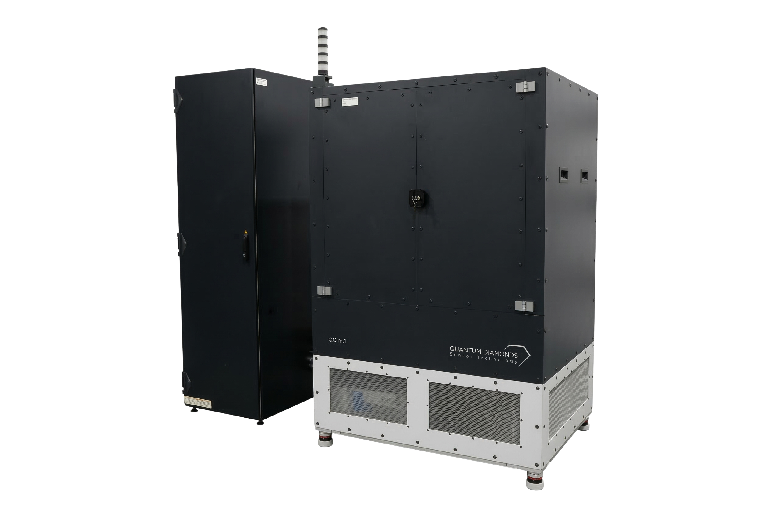
QDm.1: The Flagship Quantum Diamond Microscope for Failure Analysis
The QDm.1 is a powerful tool for imaging electrical activity in circuits, isolating short and open failures non-destructively.


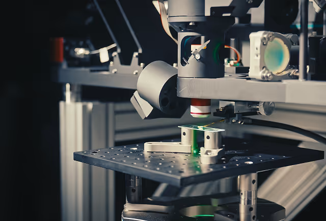
The QDm.1 enables unprecedented testing capabilities
With the our newest tool iteration, testing got even easier and precise.
Placement of a DUT near the objective, and micropositioners on the stage.
“Last updated: June 2025. An up-to-date version will be uploaded in July 2026. ”
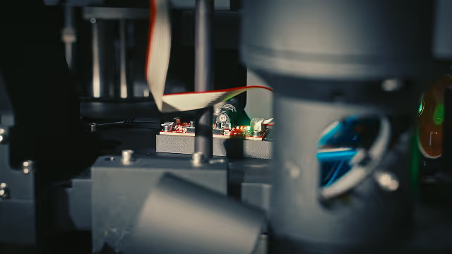
Placement of the quantum diamond sensor on the DUT with the help of a tweezer.
“Last updated: June 2025. An up-to-date version will be uploaded in July 2026. ”
Stage movement upwards to focus on the quantum diamond sensor for measurements.
“Last updated: June 2025. An up-to-date version will be uploaded in July 2026. ”
Contacting the DUT with micropositioners.
“Last updated: June 2025. An up-to-date version will be uploaded in July 2026. ”
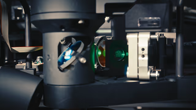
Alignment of microwave antenna on top of the sample for driving the NV centers in the quantum diamond sensor.
“Last updated: June 2025. An up-to-date version will be uploaded in July 2026. ”
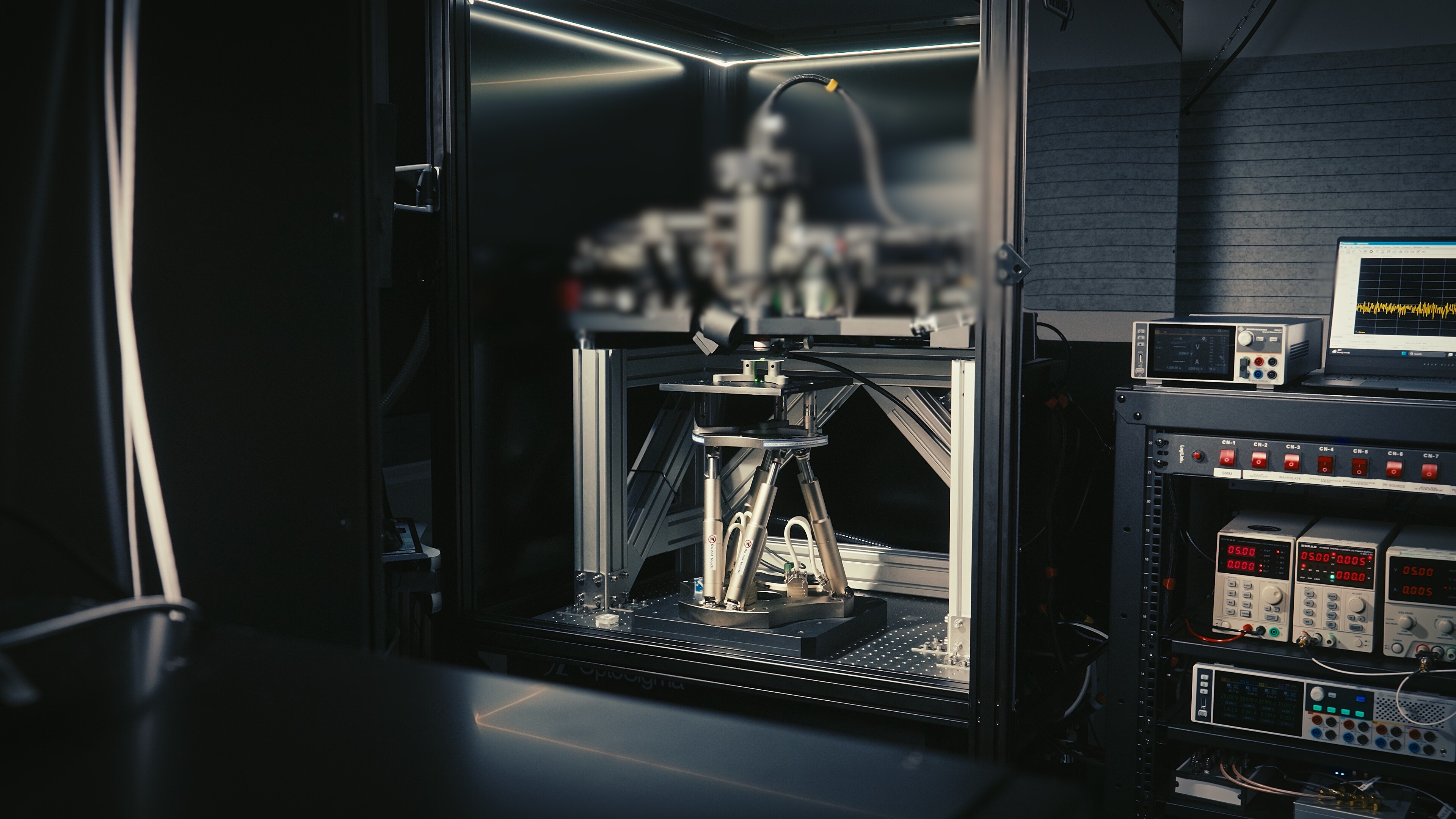
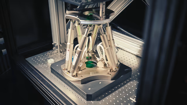
Showcase of the 6-axis high accuracy, high precision hexapod stage.
“Last updated: June 2025. An up-to-date version will be uploaded in July 2026. ”
Frequently Asked Questions (FAQ)
Prerequisites & sample preparation
For most applications, yes. Similar to LIT or OBIRCH, the device must be under failing bias conditions. In addition, the QDm.1 includes a built-in antenna that enables inductive, non-contact biasing. This feature is still experimental, but it shows promise for applications where contact is not feasible, such as cleaved wafers without pads or interposers.
Our equipment provides maximum flexibility. Customers can utilize micro-positioners for simultaneous probing and measurement from the top side or employ their drop-in sockets for BGA-side biasing with top-side measurement. The system also supports soldered parts, wire bonding, card-edge connectors, and re-wired PCB evaluation boards using standard cables.
While micropositioner probing from below is not a default feature due to the required stage opening, this capability can be integrated through minor adjustments to the base system.
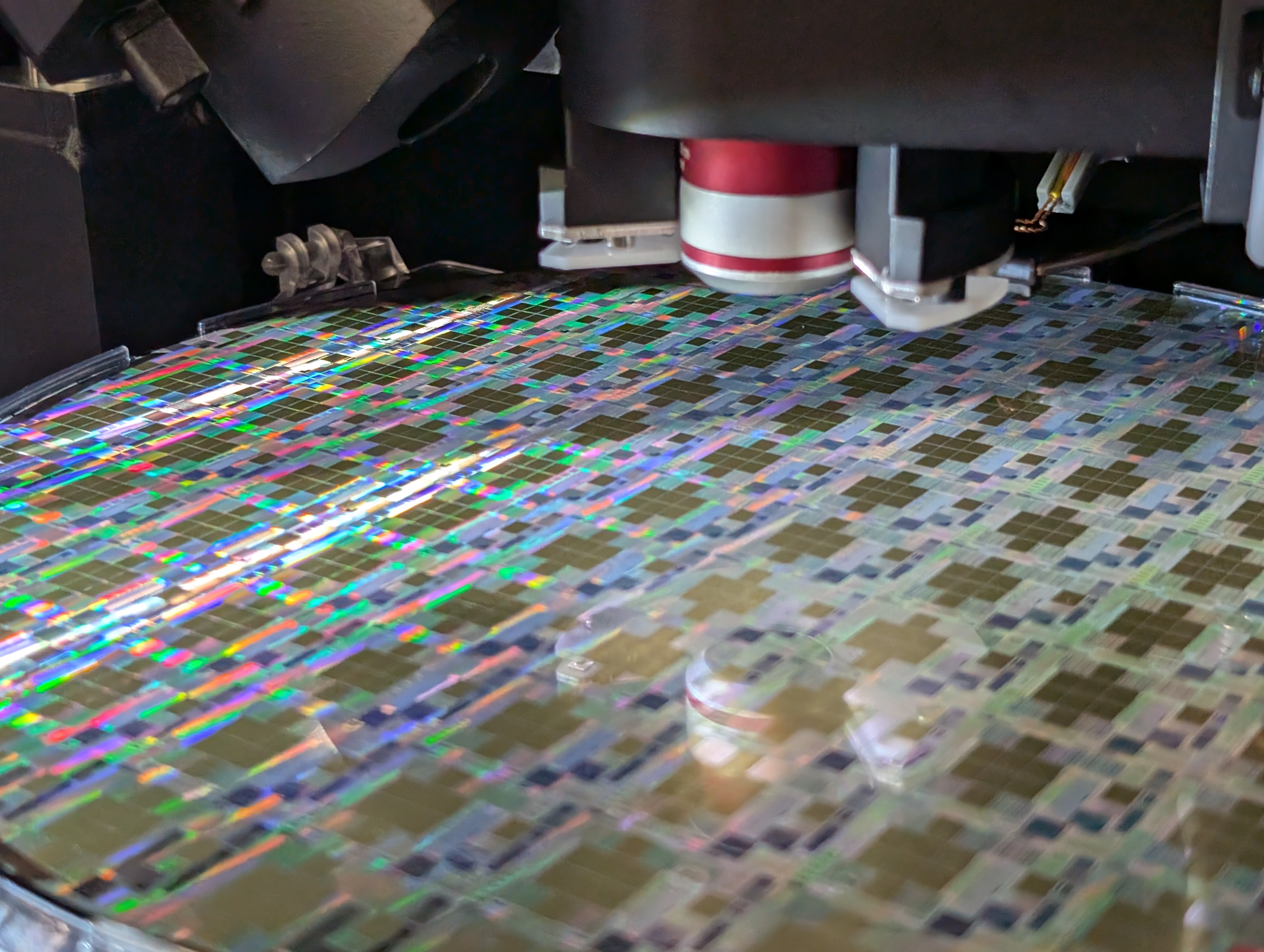
Currently, a diamond sensor of sizes (1x1 mm2, 2x2 mm2, or 4x4 mm2) is directly placed on top of a region of interest with the help of a tweezer or a suction pen.
Future integration will incorporate the diamond into the objective lens for wide-field scanning eliminate manual placement.
QDM offers FA capabilities across different sample thicknesses. XY and Z resolutions depend on the distance from the sensor to the depth of interest. Given sufficient current runs at a distance, it is within the sensitivity range; sample preparation depends on the resolution requirement from the customer side.
Some examples:
- Trying to find a short in an HBM stack of 4 dice? => Measure over the package for initial hotspot, then thin down to increase resolution if needed?
- BGA-side analysis for RDLs? => Directly place the sensor on the BGA side with no sample prep.
- Logic IC short in the metal line? => Directly place the sensor on the top side with no need to thin Si unless the layer is 100 µm+ away.
For baseline, surface roughness and tilt are tolerated up to a deviation of 10 mRads. This means: "a relatively flat surface" with no tilt visible to the naked eye or through optical microscopes is sufficient. For rougher surfaces with much surface topology, software correction is necessary and is an additional feature.
Measurement Capabilites
The largest FoV of the QDm.1 equipment is 3 mm x 3 mm for one-shot measurements.
The QDm.1 is a wide-field quantum diamond microscope that illuminates and collects information from the whole FoV simultaenously.
Only one 4x objective is used. Resolution is limited by the camera pixel size, not magnification. Future iterations could have higher magnification for higher resolution optical overlay.
Generally, not for QDM measurements. Being a magnetic imaging technique, the QDM is usually resolution-limited by the distance-to-sensor and not the magnification or pixel size. For a class of surface defects, magnification would improve resolution.
For power devices (hundreds of mA), measurements can take a few seconds. For low-current measurements down to the nA range (leakage), the process can take between 20 minutes and 2 hours.
The QDm. 1 has stitching functionality in the SW that allows the users to cover larger areas. It is not possible to do an overview scan larger than 3 mm x 3 mm in one shot.
GDS data upload and navigation is an upcoming SW feature.
The QDm.1 doesn't have an IR source or camera. However, the equipment can capture optical images for overlay because the diamond sensor is optically transparent. Future iterations will have the capability to also take IR images.
Use Cases
A broad range of defects is detectable with QDm.1 such as: metal shorts, leakages, power device oxide issues, RDL shorts, and metal opens. Our equipment is also effective for detecting high-ohmic opens and low-ohmic shorts.
The depth of reach depends on the signal that is travelling at a certain layer. As an example, mA-level currents are detectable from 700 µm+ away, while for nA-level signals, the sensor would need to be placed within 10 µm distance.
The most difficult materials to work with are ferromagnetic or paramagnetic materials, sometimes found in UBMs, such as Nickel.