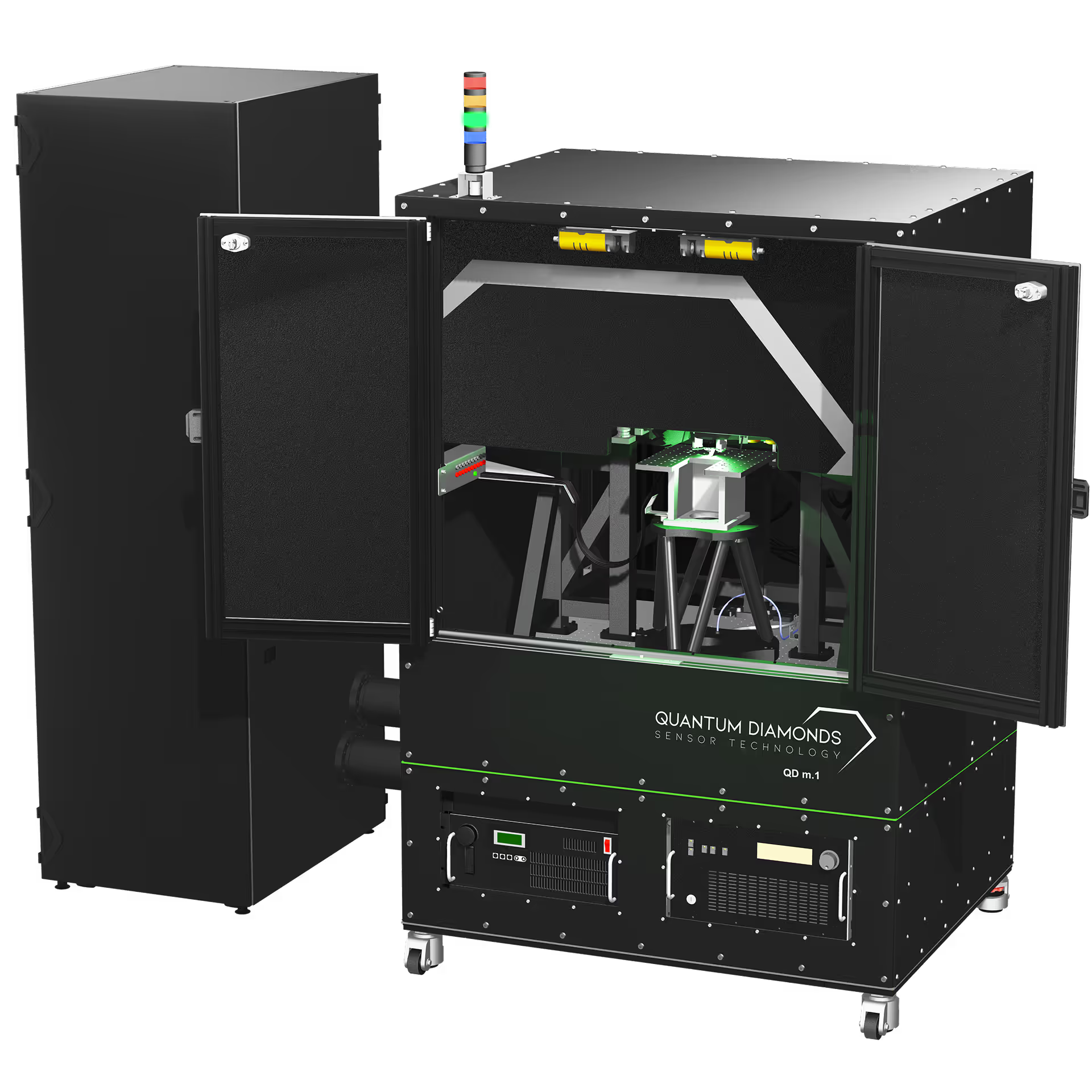
QDm.1: The Flagship Quantum Diamond Microscope for Failure Analysis
The QDm.1 is a powerful tool for imaging electrical activity in circuits, isolating short and open failures non-destructively.

Native QD software, designed for failure analysis engineers.
Our unique software interface puts advanced quantum sensing at your fingertips with an intuitive, powerful UX designed for semiconductor failure analysis and metrology teams.
Auto-Calibration and Intuitive Control
Intuitive measurements with seamless navigation, flexible controls, and smart self-calibration for users of all levels.
Interactive Data and Annotations
Access all data components simultaneously or individually. Draw, annotate, mark data freely and export in various data formats.
Overlay Visualization
Overlay your analysis data on different adjacent data such as optical and Infrared images, as well as hotspot data.
Large Area Stitching
5 cm x 5 cm travel range to stitch larger images without sample replacement.
Current Density Reconstruction
Convert your magnetic field data into electrical activity with Machine Learning enhanced 3D interactive visualization and cross-section views for deeper, actionable insights.
Precise Fault Detection
.png)
In-Lab
Commercially available, reach out for more information
High-resolution, non-destructive localization of defects at the single-chip level for R&D and failure analysis.

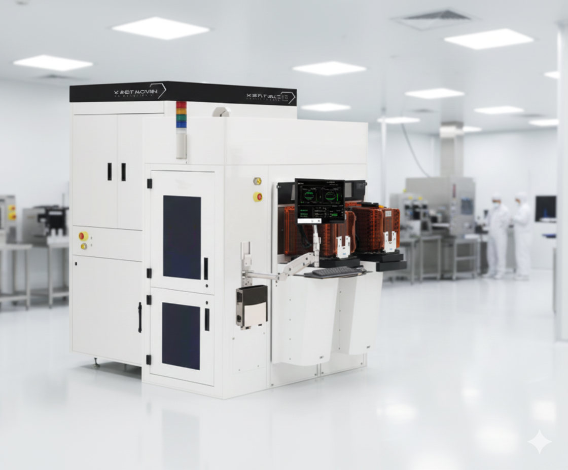
In-Line
Under development, reach out for early access
High-throughput wafer mapping for real-time yield monitoring and optimization of production processes.
Experience QDM First-Hand
Purchase the QDm.1, a powerful tool for imaging electrical activity in circuits and non-destructively isolating short and open failures. Or join our exclusive demo program today to see the system in action at your facility.
